PCB Trace Repair for Beginners: A Hobbyist's Guide to Saving Damaged BoardsAuthor : Adrian September 05,smt solder paste mixer 2025Table of ContentsIf you're a hobbyist wondering how to fix a damaged printed circuit board (PCB) without breaking the bank or needing fancy tools, you're in the right place. PCB trace repair can seem intimidating, but with the right approach, it's entirely possible to perform easy PCB trace repairat home. In this guide, we'll walk you through DIY PCB trace repairtechniques that are beginner-friendly, focusing on PCB trace repair at home, PCB trace repair without special equipment, and cheap PCB trace repair methods. Whether it's a broken trace on a favorite gadget or a project board, you'll learn how to bring it back to life step by step.
Why PCB Trace Repair Matters for HobbyistsPCBs are the backbone of almost every electronic device, from smartphones to DIY Arduino projects. The tiny copper lines, or traces, on these boards carry electrical signals between components. When a trace gets damaged—due to physical stress, overheating, or corrosion—the circuit can fail, rendering the device useless. For hobbyists, replacing a damaged board can be expensive or impractical, especially for one-off projects. Learning easy PCB trace repairsaves money, extends the life of your electronics, and boosts your troubleshooting skills.
Understanding PCB Traces and Common DamageBefore diving into repair methods, let's break down what PCB traces are and how they get damaged. Traces are thin copper pathways etched onto the board's surface, typically 1-2 mils (0.001-0.002 inches) thick, though this varies by design. They connect components like resistors, capacitors, and ICs, ensuring signals flow with minimal resistance—often in the range of milliohms per inch for standard copper traces. Common causes of trace damage include:
Identifying the type of damage is the first step in DIY PCB trace repair. A visual inspection often reveals cracks, burns, or complete breaks in the copper line.
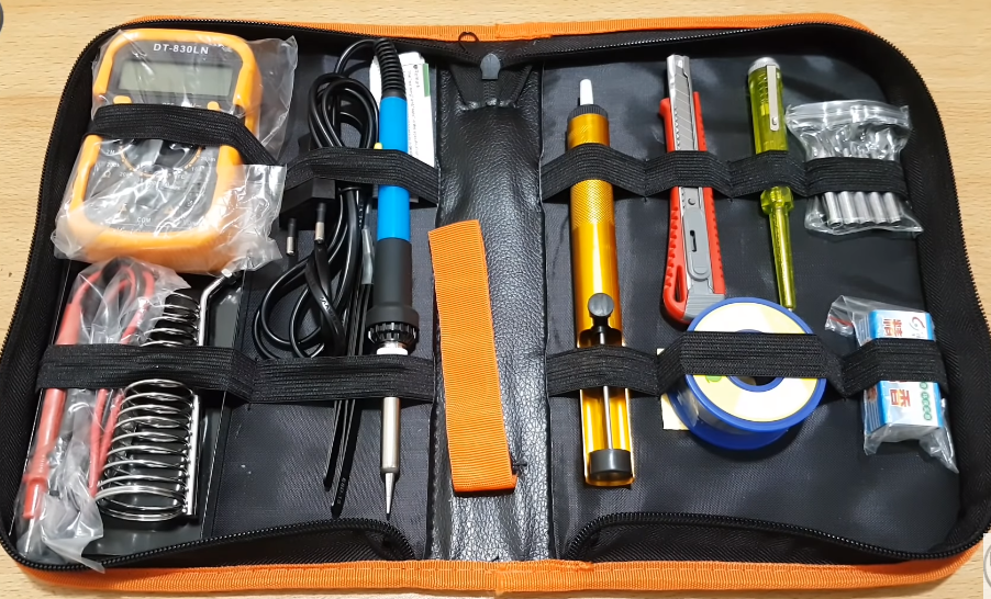
Tools and Materials for PCB Trace Repair at HomeOne of the best parts about PCB trace repair without special equipmentis that you likely already have most of the tools needed. Here's a list of basic items for cheap PCB trace repair methods:
These tools keep costs low and make PCB trace repair at homeaccessible to beginners. No need for expensive rework stations or professional gear!
Step-by-Step Guide to Easy PCB Trace RepairNow, let's get into the practical steps for DIY PCB trace repair. We'll cover two main methods that cater to beginners using minimal tools: repairing with a jumper wire and using conductive ink. Follow these steps carefully for the best results. Step 1: Safety FirstAlways work on a powered-off device. Unplug the board from any power source and discharge any capacitors by shorting their leads with an insulated tool. Work in a well-ventilated area when soldering to avoid inhaling fumes. Step 2: Inspect and Identify DamageUse a magnifying glass to locate the broken trace. Look for visible cracks, burns, or areas where the copper is missing. If the trace is covered by a green solder mask, gently scrape it away with a utility knife to expose the copper. Be careful not to cut too deep and damage nearby traces. Step 3: Clean the AreaDip a cotton swab in isopropyl alcohol (at least 90% concentration) and clean the damaged area. Remove dirt, flux residue, or oxidation from the copper to ensure a good connection during repair. Let the board dry completely before proceeding. Method 1: Repairing with a Jumper Wire (For Larger Breaks)This is one of the most reliable cheap PCB trace repair methodsfor complete breaks or wide gaps in traces. Here's how to do it:
This method works well for traces carrying up to 1-2 amps, as 30 AWG wire can handle that current with minimal resistance (about 0.1 ohms per foot).
Method 2: Using Conductive Ink (For Minor Damage)For hairline cracks or very small breaks, a conductive ink pen offers an easy PCB trace repairsolution. These pens contain silver or carbon-based ink that conducts electricity. Here's the process:
Conductive ink is less durable than soldering and typically handles lower currents (under 0.5 amps), so use it for signal traces rather than power lines. Step 4: Test the RepairAfter completing the repair, use a multimeter set to continuity mode to check if the trace is conducting properly. Place the probes on either side of the repaired section. A beep or low resistance reading (under 1 ohm for short traces) indicates success. If there's no continuity, recheck your connections or apply more solder/ink as needed.
Tips for Successful PCB Trace Repair Without Special EquipmentTo ensure your PCB trace repair at homegoes smoothly, keep these pointers in mind:
Common Mistakes to Avoid in DIY PCB Trace RepairEven with cheap PCB trace repair methods, beginners can run into pitfalls. Here's what to watch out for:
When to Seek Professional HelpWhile PCB trace repair without special equipmentworks for many scenarios, some damages are beyond a hobbyist's scope. If the board has multiple layers (common in modern electronics) and the broken trace is internal, home repair won't cut it. Similarly, if the damage affects critical components or high-voltage circuits, it's safer to consult a professional to avoid risks like electrical hazards or further damage.
Conclusion: Mastering Easy PCB Trace RepairRepairing a damaged PCB doesn't have to be daunting or expensive. With the techniques outlined in this guide, you can tackle easy PCB trace repairusing everyday tools and minimal investment. Whether you opt for a jumper wire or conductive ink, DIY PCB trace repairempowers you to save your projects and learn valuable skills along the way. By following these steps for PCB trace repair at home, using cheap PCB trace repair methods, and avoiding common mistakes, you'll be well on your way to reviving broken boards like a pro. Remember, practice makes perfect. Start with small repairs, build your confidence, and soon you'll handle even trickier fixes with ease. Your wallet—and your gadgets—will thank you for mastering PCB trace repair without special equipment.
 The Role of Flux in PCB Wave Soldering: Selection, Application, and Residue RemovalMarch 16, 2026PCB wave soldering flux types include rosin, water-soluble, and no-clean options with varying activity levels for oxide removal and solder flow. This guide covers selection criteria, spray foam drop-jet application methods, residue removal processes, and alternatives like nitrogen blanketing to boost joint reliability and yields for engineers. Article Achieving Uniform Solder Fillets in PCB Wave Soldering: Process ControlMarch 16, 2026Achieve uniform solder fillets in PCB wave soldering with process control strategies. Optimize flux, preheat, wave height, conveyor speed for consistent fillet shape, height, and wetting balance. Includes visual inspection tips and troubleshooting for reliable through-hole assemblies. Boost quality in production. Article Optimizing Conveyor Speed for Efficient PCB Wave SolderingMarch 16, 2026Learn PCB wave soldering conveyor speed calculation to manage dwell time, immersion depth, and throughput effectively. Electric engineers get practical steps, best practices, and troubleshooting tips for higher process efficiency and fewer defects in wave soldering operations. Article Understanding IPC Standards for PCB Surface Finishes: Ensuring Quality and ComplianceMarch 11, 2026Understand IPC standards IPC 4552 ENIG and IPC 4553 immersion silver for PCB surface finishes. Ensure compliance, enhance solderability, and prevent common defects to achieve reliable, high quality circuit boards. Article Miniaturization Challenges in PCB AssemblyMarch 11, 2026Navigate the complexities of high density interconnect PCB assembly and precise component placement. Learn to tackle miniaturization challenges, from tiny part handling to thermal stress, ensuring robust and reliable electronics. Article High Speed Routing Techniques: PCBMarch 11, 2026Master high speed routing in PCBs to ensure signal integrity and minimize electromagnetic interference. Learn essential techniques for robust designs, from controlled impedance to differential pair strategies. Prevent performance issues and achieve reliable electronics. ArticleGet Instant PCB |